Context:
This Article is based on the news “How India’s first semiconductor fabrication plant can help plug in to global value chain” which was published in the Indian Express. The Union Cabinet recently approved three chip-related projects, including India’s first semiconductor fabrication plant.
India Approves Tata Group’s Ambitious Semiconductor Projects in Gujarat and Assam – The three projects are:
-
Semiconductor Plant in Dholera, Gujarat:
- The semiconductor plant is a collaboration between Tata Group and Taiwanese foundry Powerchip Semiconductor Manufacturing Corp (PSMC).
- It will provide access to leading-edge and mature nodes including 28 nanometer, 40 nm, 55 nm, 90 nm and 110 nm.
- Capacity of 50,000 wafers per month.
-
Chip Assembly plant in Morigaon, Assam:
- The Tata Group will also set up a chip assembly plant with a capacity to manufacture 48 million chips per day, and will primarily cater to export needs.
-
Chip Packaging Facility in Sanand, Gujarat:
-
- A chip packaging facility in Gujarat’s Sanand was also approved by the Cabinet.
About Semiconductors: The Tiny Powerhouses Driving Modern Electronics
- Semiconductors, often called ‘chips,’ are tiny electronic circuits containing transistors, diodes, capacitors, resistors, and interconnections.
- These circuits are intricately arranged on a silicon wafer.
- Semiconductors are employed in the manufacture of various kinds of electronic devices, including diodes, transistors, and integrated circuits. Such devices have found wide application because of their compactness, reliability, power efficiency, and low cost.
About the Semiconductors Industry
- Success in the semiconductor industry depends on creating smaller, faster, and cheaper products.
- The more transistors on a chip, the faster it can do its work.
- This creates fierce competition in the industry and new technologies lower the cost of production per chip.
- Therefore, semiconductor companies need to maintain large research and development budgets.
- The semiconductor industry is highly competitive, with major players from countries like the United States, China, South Korea, and Taiwan dominating the market.
- However, in recent times, India has emerged as a rising star in the industry.
|
Some Terms Associated With Semiconductor Industry:
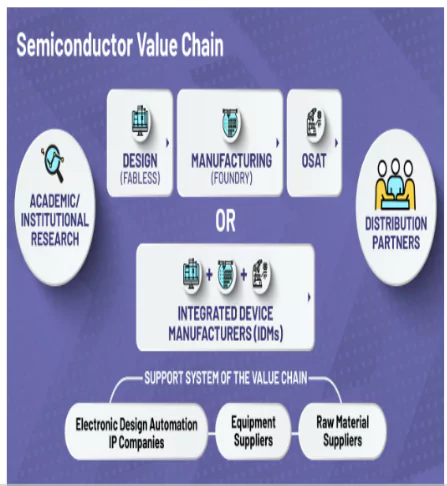
- Wafers: The flat round disk of silicon in which chips are built on.
- Fab: Short for “fabrication”, which means “manufacturing” or “making”. The fab is where the semiconductors are made. Fab facilities specialize in printing these miniature circuits onto silicon wafers according to chip designs.
- Transistors: The tiny devices built into the computer chips that do all of the calculations. There can be billions of transistors on a single computer chip.
- Foundry: A semiconductor manufacturing facility that produces integrated circuits (ICs) based on designs provided by external companies.
- Fabless: A business model where a semiconductor company designs and markets ICs but outsources their fabrication to third-party foundries.
- Integrated Device Manufacturer (IDM): A company that both designs and manufactures its own semiconductor devices, encompassing the entire supply chain.
- Outsourced Semiconductor Assembly and Test (OSAT): This is a third-party service that suppliers around the world offer, which consists, as the name implies, of semiconductor assembly, packaging and testing of ICs (Integrated Circuits).
|

India’s Semiconductor State of Play and Market Opportunities:
- Rapidly Expanding Market Size: According to a report from India Electronics and Semiconductor Association (IESA), India’s semiconductor consumption is expected to reach $64 billion by 2026.
- Desires to Expand its Manufacturing Capabilities: India is currently strongest in the R&D and design facets of the semiconductor value chain
- More recently, India has turned its attention to semiconductor fabrication (“fabs”) and post-production assembly, test, and packaging (ATP), where semiconductors are tested and assembled into sophisticated packages
- (Image shows Semiconductor Value Chain ecosystem)
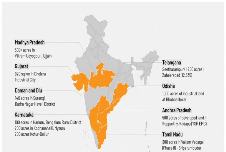
Potential Clusters for the Setting up of Fabs:

The Indian government will collaborate with state governments to establish High-Tech Clusters with essential infrastructure:
- Land: Adequate land for fab facilities.
- Semiconductor-Grade Water: High-quality water meeting semiconductor manufacturing standards.
- Power: Reliable and high-quality power supply.
- Logistics: Efficient transportation and logistics.
- Research Ecosystem: Support for R&D and innovation.
- Identified Special Economic Zones (SEZ’s) can prove suitable locations.
Fostering India’s Semiconductor Ecosystem: Government Initiatives and Policy Frameworks
- National Policy on Electronics (NPE): India has launched the National Policy on Electronics (NPE) in 2019, with the aim of creating a globally competitive electronics manufacturing industry in the country.
- Semicon India Program: The Union Cabinet had also approved the Semicon India Program, with an outlay of INR 76,000 crore for the development of a sustainable semiconductor and display manufacturing ecosystem in India.
-
About India Semiconductor Mission (ISM):
- ISM was launched in 2021 under the aegis of the Ministry of Electronics and IT (MeitY) for the development of a sustainable semiconductor and display ecosystem in the country.
- Components:
- Scheme for setting up of Semiconductor Fabs in India:
- Scheme for setting up of Display Fabs in India
- Scheme for setting up of Compound Semiconductors / Silicon Photonics / Sensors Fab and Semiconductor Assembly, Testing, Marking and Packaging (ATMP) / OSAT facilities in India
- Design Linked Incentive (DLI) Scheme: It offers financial incentives, design infrastructure support across various stages of development and deployment of semiconductor design for Integrated Circuits (ICs), Chipsets, System on Chips (SoCs), Systems & IP Cores and semiconductor linked design.
- Foreign Direct Investment (FDI) Norms: 100% FDI is allowed under the automatic route.
- The “Make in India” campaign and the Electronics Manufacturing Cluster (EMC) scheme aim to attract investments and promote semiconductor manufacturing in the country.
|
Empowering India: The Strategic Significance of Semiconductor Fabrication in Dholera
- Reducing Dependence on Imports: 70% of the current global manufacturing capacity is confined to South Korea, Taiwan and China, with the US and Japan making up for much of the rest.
- By having our own fab, India can enhance its self-sufficiency in semiconductor production.
- Balance Trade Deficits: India runs a large trade deficit in semiconductor products. An estimated 70 percent of India’s electronics imports come from China and Hong Kong, with an additional 13 percent coming from Singapore.
- Intricate Fabrication Process: Semiconductor fabrication involves intricate steps, including clean rooms to prevent contamination. The process requires inputs like silicon wafers, specialty chemicals, and an uninterrupted power supply. A domestic fab ensures control over these critical components
- Boost Manufacturing Sector: This ‘fab’ will have manufacturing capacity of up to 50,000 wafers per month.
- This can ensure a steady supply of the components needed for future technologies.
- Create Job Opportunities: It has the potential to create direct employment of 20,000 advanced technology jobs and about 60,000 indirect jobs in high-tech sectors.
- Comparative Advantage: It will offer India leverage in the chip wars by increasing its say in the geopolitics of technology that has so far been shaped by China and the United States.
- Resilience in Global Supply Chain: Diversifying Manufacturing will help strengthen the supply chain of semiconductors globally.
- Example: China’s Semiconductor Manufacturing International Corporation (SMIC) is currently facing challenges in acquiring advanced chip-making equipment. This difficulty stems from a blockade led by the United States, restricting the supply of crucial technology to SMIC.
- Spillover Effects: Semiconductor manufacturing can produce tremendous spillover and “learning by doing” effects across the rest of India’s high-tech economy.
Challenges in Boosting Domestic Semiconductor Sector:
- Lack of Fabrication Units: In India, more than 90% of global companies already have their R&D and design centres for semiconductors but never established their fabrication units.
- Although India has semiconductor fabs in Mohali and Bangalore, they are purely strategic for defence and space applications only.
- Resource-Intensive Chip Production: Chip-making also requires gallons of ultrapure water in a single day.
- An uninterrupted supply of power is central to the process, with just seconds of fluctuations or spikes causing millions in losses.
- Lack of Engagement from Market Players: Due to complicated application process, and lack of pre-existing ecosystem.
- Example- In 2021, India launched a $10 billion incentive program to attract chipmakers and display manufacturers. The initiative offered up to 50% of capital expenditures as incentives to companies establishing local manufacturing projects. It was modified due to lacklustre engagement.
- High Capital Extensive and Entry Barriers:
- Semiconductors are highly complex products to design and manufacture.
- Level of investment in both R&D and capital expenditure is huge thereby making semiconductor fabrication an extremely capital intensive business with high entry barriers.
- Closed Ecosystem: The global semiconductor chip industry is dominated by some countries and a handful of companies.
- Taiwan and South Korea make up about 80% of the global foundry base for chips.
- Insufficient incentives provided by India: The US and EU have rolled out more lucrative incentive schemes than India.
- Insufficient Talent Pool: The engineers graduating in India annually could help, but better courses, training, and preparedness are needed, as only a small fraction are industry ready upon graduation.
- Limited Original Research in Semiconductor Design: The future of the chip is decided by original research.
- The government, however, is aware of that shortcoming and is in the process of setting up a R&D lab at Semiconductor Laboratory (SCL) in Mohali.
- Multiple Clearances Needed: Fabs use sub-5 nanometer technology that requires clearance from both the technology provider and the Government, adding complexity to the establishment process.
Way Forward
- Conducive Environment: India has the potential to play a much more significant role in global semiconductor value chains, provided the government upholds its investment policies, maintains a conducive regulatory and business environment, and avoids measures that create unpredictability.
- Changing the Focus towards OSAT: Companies that specialise in Outsourced Semiconductor Assembly and Test (OSAT) are less expensive to set up, and generate better margins.
- The OSAT set-ups take care of the less capital-intensive parts of chipmaking, such as assembling the precise components that have already been manufactured, and running specialised tests to approve them.
- Collaborative Efforts: If like-minded nations each specialise in different aspects of the semiconductor and electronics manufacturing process, and work together on assembly and distribution, that can also solve the geopolitical problem of Chinese dominance.
- Focus on Design and Research and Development: The initial funding should focus on areas like design and R&D, for which India already has an established talent pool.
![]() 1 Mar 2024
1 Mar 2024


