ASML Unveils Cutting-Edge High NA EUV Lithography Machine

7 Mar 2024

Context:

  • Recently ASML unveiled its new ‘High NA EUV’ Lithography machines which represent the cutting edge in semiconductor manufacturing, revolutionising the production of these essential components.

High NA EUV Lithography Machine

  • High NA EUV Machine: It uses extreme ultraviolet (EUV) photolithography, a next-generation technology, to make the semiconductors.
  • Process: The mould of the circuits of a transistor, a type of semiconductor, is transferred to a silicon wafer coated with a light-sensitive material called a photoresist.
  • Rayleigh scattering criterion: According to this criterion, the size of the feature to be projected on the wafer is proportional to the wavelength of light used and inversely proportional to the lens’s aperture that collects light before projecting it onto the wafer.

About Lithography:

  • Lithography: A crucial step in semiconductor fabrication, lithography involves transferring intricate patterns from a mask or photomask onto the wafer surface using light exposure and photoresist materials.

Steps in Photolithography:

  • Substrate Cleaning: The substrate (typically a silicon wafer) is cleaned to eliminate pollutants.
  • Photoresist Covering: A slight layer of photoresist is turned covered onto the substrate, making an even surface.
  • Lithography
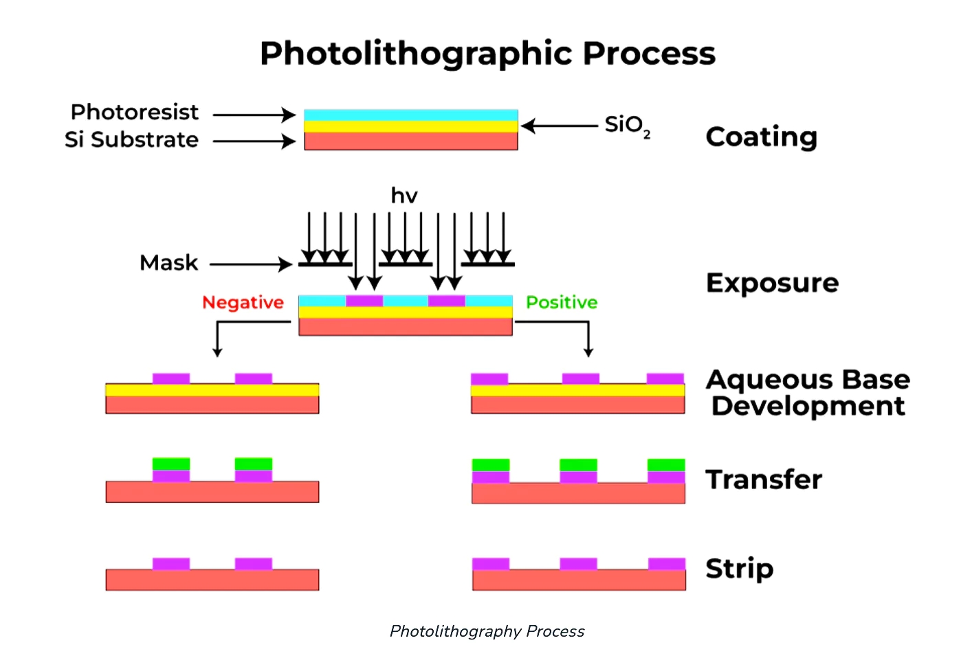
Soft Bake: The coated substrate is gently heated to eliminate solvent and guarantee uniformity.
  • Mask Alignment: A photomask with the desired pattern is aligned over the substrate.
  • Exposure: UV light is radiated through the veil onto the photoresist, causing a substance change.
  • Post-Exposure Bake: The substrate is warmed again to balance out the example in the photoresist.
  • Development: The exposed photoresist is removed using a developer solution, revealing the pattern.
  • Hard Bake: The remaining photoresist is made more durable by performing a final heating step.
  • Etching or Implantation: The uncovered substrate regions are carved or adjusted depending on the situation.
  • Photoresist Stripping: The patterned substrate is left behind after removing the remaining photoresist.
Photoresists
Photoresists are essentially hydrocarbon polymers composed of a novol-ack resin, a photoactive compound and an organic solvent. 

Advantages of Photolithography

  • High-Quality Patterns: Photolithography creates precise and detailed patterns on various surfaces like computer chips.
  • Efficient Production: It’s effective in mass production, like the production of computer chips in a factory.
  • Cost-Effective: It is relatively affordable to make more items, after the initial setup.
  • Versatile: It can be used with different materials, including metals and plastics.
  • Accurate Alignment: It ensures that all parts fit together correctly.
  • Fast Processing: It enhances the pace of machine working, thus increasing production speed.

Applications of Photolithography

  • Semiconductor Manufacturing: Photolithography is essential for creating components on computer chips.
  • Electronics: It makes sensors, Mobile-LED TV displays, and other electronic components.
  • Circuit Boards: It helps define electricity pathways in circuit boards.
  • Optics: It is used to produce lenses and optical devices.
  • Medical Devices: Production of medical devices in diagnosis and Treatment.
  • Nanotechnology: It has applications in Nano-technology,
Also Read: India’s First Semiconductor Fabrication Plant

News Source: The Hindu

Must Read
NCERT Notes For UPSC UPSC Daily Current Affairs
UPSC Blogs UPSC Daily Editorials
Daily Current Affairs Quiz Daily Main Answer Writing
UPSC Mains Previous Year Papers UPSC Test Series 2024


Archive Calendar

Mon Tue Wed Thu Fri Sat Sun
 123
45678910
11121314151617
18192021222324
25262728293031

Need help preparing for UPSC or State PSCs?

Connect with our experts to get free counselling & start preparing

Know about Physics Wallah

Physics Wallah is an Indian online education platform, that provides accessible & comprehensive learning experiences to students of classes 6 to 12 and those preparing for JEE and NEET exams. We also provide extensive NCERT solutions, sample papers, NEET, JEE Mains, BITSAT previous year papers, which makes us a one-stop solution for all resources. Physics Wallah also caters to over 3.5 million registered students and over 78 lakh+ Youtube subscribers with 4.8 rating on its app.

We Stand Out because

We successfully provide students with intensive courses by India's qualified & experienced faculties. PW strives to make the learning experience comprehensive and accessible for students of all sections of society. We believe in empowering every single student who couldn't dream of a good career in engineering and medical field earlier.

Our Key Focus Areas

Physics Wallah’s main focus is to create accessible learning experiences for students all over India. With courses like Lakshya, Udaan, Arjuna & many others, we have been able to provide a ready solution for lakhs of aspirants. From providing Chemistry, Maths, Physics formulae to giving e-books of eminent authors, PW aims to provide reliable solutions for student prep.

What Makes Us Different

Physics Wallah strives to develop a comprehensive pedagogical structure for students, where they get a state-of-the-art learning experience with study material and resources. Apart from catering students preparing for JEE Mains and NEET, PW also provides study material for each state board like Uttar Pradesh, Bihar, and others.

Aiming for UPSC?

Download Our App

# #
Quick Revise Now !
AVAILABLE FOR DOWNLOAD SOON
UDAAN PRELIMS WALLAH
Comprehensive coverage with a concise format
Integration of PYQ within the booklet
Designed as per recent trends of Prelims questions
हिंदी में भी उपलब्ध
Quick Revise Now !
UDAAN PRELIMS WALLAH
Comprehensive coverage with a concise format
Integration of PYQ within the booklet
Designed as per recent trends of Prelims questions
हिंदी में भी उपलब्ध

<div class="new-fform">


    </div>

    Subscribe our Newsletter
    Sign up now for our exclusive newsletter and be the first to know about our latest Initiatives, Quality Content, and much more.
    *Promise! We won't spam you.
    Yes! I want to Subscribe.