Win up to 100% Scholarship

Register Now

ASML Unveils Cutting-Edge High NA EUV Lithography Machine

Context:

  • Recently ASML unveiled its new ‘High NA EUV’ Lithography machines which represent the cutting edge in semiconductor manufacturing, revolutionising the production of these essential components.

High NA EUV Lithography Machine

  • High NA EUV Machine: It uses extreme ultraviolet (EUV) photolithography, a next-generation technology, to make the semiconductors.
  • Process: The mould of the circuits of a transistor, a type of semiconductor, is transferred to a silicon wafer coated with a light-sensitive material called a photoresist.
  • Rayleigh scattering criterion: According to this criterion, the size of the feature to be projected on the wafer is proportional to the wavelength of light used and inversely proportional to the lens’s aperture that collects light before projecting it onto the wafer.

About Lithography:

  • Lithography: A crucial step in semiconductor fabrication, lithography involves transferring intricate patterns from a mask or photomask onto the wafer surface using light exposure and photoresist materials.

Steps in Photolithography:

  • Substrate Cleaning: The substrate (typically a silicon wafer) is cleaned to eliminate pollutants.
  • Photoresist Covering: A slight layer of photoresist is turned covered onto the substrate, making an even surface.
  • Lithography
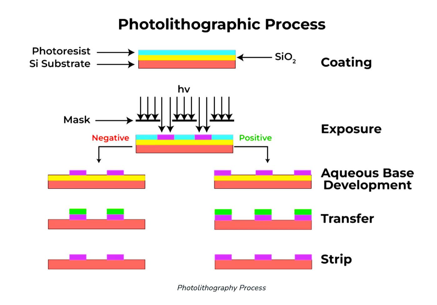
Soft Bake: The coated substrate is gently heated to eliminate solvent and guarantee uniformity.
  • Mask Alignment: A photomask with the desired pattern is aligned over the substrate.
  • Exposure: UV light is radiated through the veil onto the photoresist, causing a substance change.
  • Post-Exposure Bake: The substrate is warmed again to balance out the example in the photoresist.
  • Development: The exposed photoresist is removed using a developer solution, revealing the pattern.
  • Hard Bake: The remaining photoresist is made more durable by performing a final heating step.
  • Etching or Implantation: The uncovered substrate regions are carved or adjusted depending on the situation.
  • Photoresist Stripping: The patterned substrate is left behind after removing the remaining photoresist.
Photoresists
Photoresists are essentially hydrocarbon polymers composed of a novol-ack resin, a photoactive compound and an organic solvent. 

Advantages of Photolithography

  • High-Quality Patterns: Photolithography creates precise and detailed patterns on various surfaces like computer chips.
  • Efficient Production: It’s effective in mass production, like the production of computer chips in a factory.
  • Cost-Effective: It is relatively affordable to make more items, after the initial setup.
  • Versatile: It can be used with different materials, including metals and plastics.
  • Accurate Alignment: It ensures that all parts fit together correctly.
  • Fast Processing: It enhances the pace of machine working, thus increasing production speed.

Applications of Photolithography

  • Semiconductor Manufacturing: Photolithography is essential for creating components on computer chips.
  • Electronics: It makes sensors, Mobile-LED TV displays, and other electronic components.
  • Circuit Boards: It helps define electricity pathways in circuit boards.
  • Optics: It is used to produce lenses and optical devices.
  • Medical Devices: Production of medical devices in diagnosis and Treatment.
  • Nanotechnology: It has applications in Nano-technology,
Also Read: India’s First Semiconductor Fabrication Plant

News Source: The Hindu

Must Read
NCERT Notes For UPSC UPSC Daily Current Affairs
UPSC Blogs UPSC Daily Editorials
Daily Current Affairs Quiz Daily Main Answer Writing
UPSC Mains Previous Year Papers UPSC Test Series 2024


To get PDF version, Please click on "Print PDF" button.

 Final Result – CIVIL SERVICES EXAMINATION, 2023.   Udaan-Prelims Wallah ( Static ) booklets 2024 released both in english and hindi : Download from Here!     Download UPSC Mains 2023 Question Papers PDF  Free Initiative links -1) Download Prahaar 3.0 for Mains Current Affairs PDF both in English and Hindi 2) Daily Main Answer Writing  , 3) Daily Current Affairs , Editorial Analysis and quiz ,  4) PDF Downloads  UPSC Prelims 2023 Trend Analysis cut-off and answer key

THE MOST
LEARNING PLATFORM

Learn From India's Best Faculty


 Final Result – CIVIL SERVICES EXAMINATION, 2023.   Udaan-Prelims Wallah ( Static ) booklets 2024 released both in english and hindi : Download from Here!     Download UPSC Mains 2023 Question Papers PDF  Free Initiative links -1) Download Prahaar 3.0 for Mains Current Affairs PDF both in English and Hindi 2) Daily Main Answer Writing  , 3) Daily Current Affairs , Editorial Analysis and quiz ,  4) PDF Downloads  UPSC Prelims 2023 Trend Analysis cut-off and answer key

Quick Revise Now !
AVAILABLE FOR DOWNLOAD SOON
UDAAN PRELIMS WALLAH
Comprehensive coverage with a concise format
Integration of PYQ within the booklet
Designed as per recent trends of Prelims questions
हिंदी में भी उपलब्ध
Quick Revise Now !
UDAAN PRELIMS WALLAH
Comprehensive coverage with a concise format
Integration of PYQ within the booklet
Designed as per recent trends of Prelims questions
हिंदी में भी उपलब्ध

<div class="new-fform">


    </div>

    Subscribe our Newsletter
    Sign up now for our exclusive newsletter and be the first to know about our latest Initiatives, Quality Content, and much more.
    *Promise! We won't spam you.
    Yes! I want to Subscribe.